Mastering Kicad Curved Traces For Custom Pcb Designs To Improve Your Circuit Board Aesthetics And Functionality - Melting kicad
If you are looking for How to Design Coplanar Waveguide with Ground in Your PCB: Mastering you've visit to the right web. We have 35 Images about How to Design Coplanar Waveguide with Ground in Your PCB: Mastering like Mastering KiCAD: Open-Source PCB Design for Beginners | Datafloq News, Create custom pcb designs with kicad expertise by Pcbprof | Fiverr and also Raspberry Pi Pico (RP2040) Schematic & PCB Design in KiCAD – DeepBlue. Read more:
How To Design Coplanar Waveguide With Ground In Your PCB: Mastering
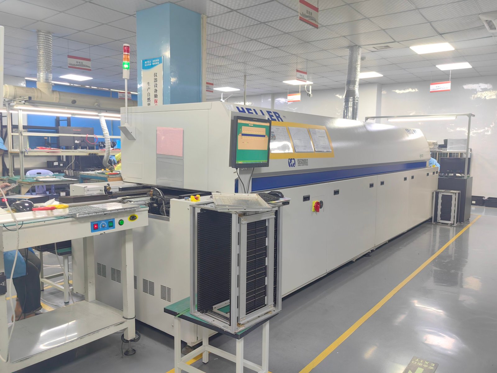 hcjm-pcba.com
How to Design Coplanar Waveguide with Ground in Your PCB: Mastering ...
Curved Traces Made With KiCad 5.99 : R/KiCad
 www.reddit.com
Curved Traces made with KiCad 5.99 : r/KiCad
How To Design Coplanar Waveguide With Ground In Your PCB: Mastering
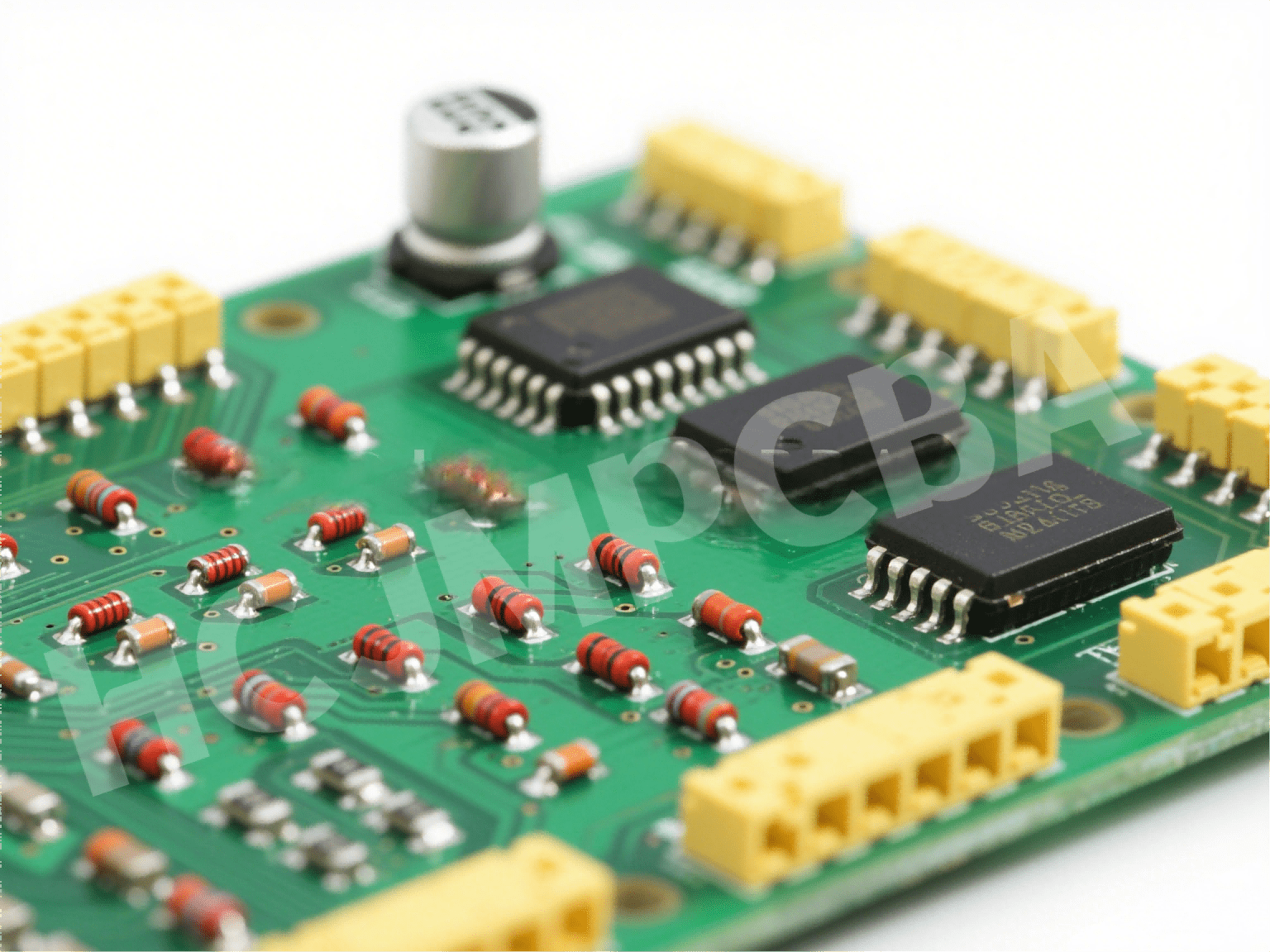 hcjm-pcba.com
How to Design Coplanar Waveguide with Ground in Your PCB: Mastering ...
PCB_ESP32 CSI Curved Traces Resources - EasyEDA
 easyeda.com
PCB_ESP32 CSI Curved traces Resources - EasyEDA
Close-up Of A Printed Circuit Board (PCB) With Intricate Pathways And
 www.dreamstime.com
Close-up of a Printed Circuit Board (PCB) with Intricate Pathways and ...
How To Design Coplanar Waveguide With Ground In Your PCB: Mastering
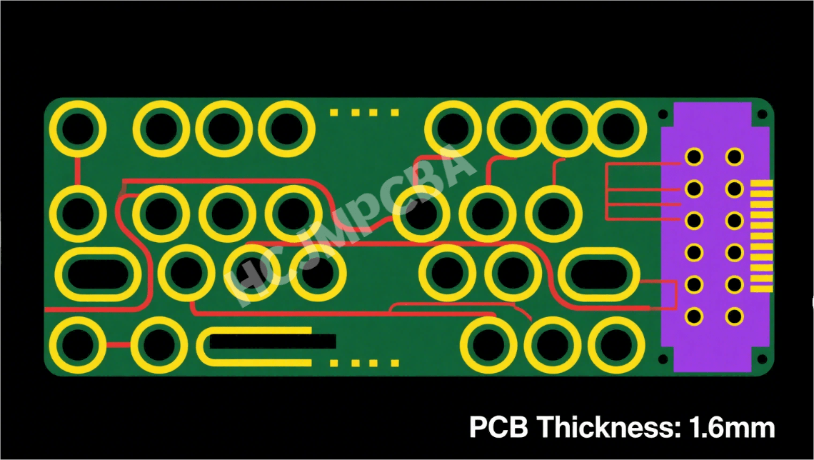 hcjm-pcba.com
How to Design Coplanar Waveguide with Ground in Your PCB: Mastering ...
How To Design Coplanar Waveguide With Ground In Your PCB: Mastering
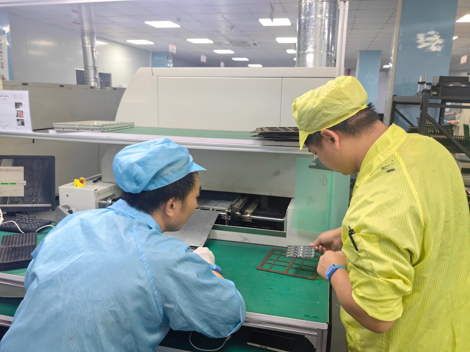
 hcjm-pcba.com
How to Design Coplanar Waveguide with Ground in Your PCB: Mastering ...
How To Design Coplanar Waveguide With Ground In Your PCB: Mastering
 hcjm-pcba.com
How to Design Coplanar Waveguide with Ground in Your PCB: Mastering ...
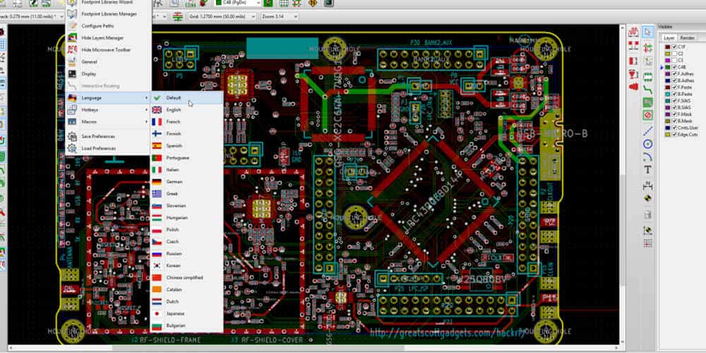
KiCad 8 Custom PCB Design Rules | SaludPCB
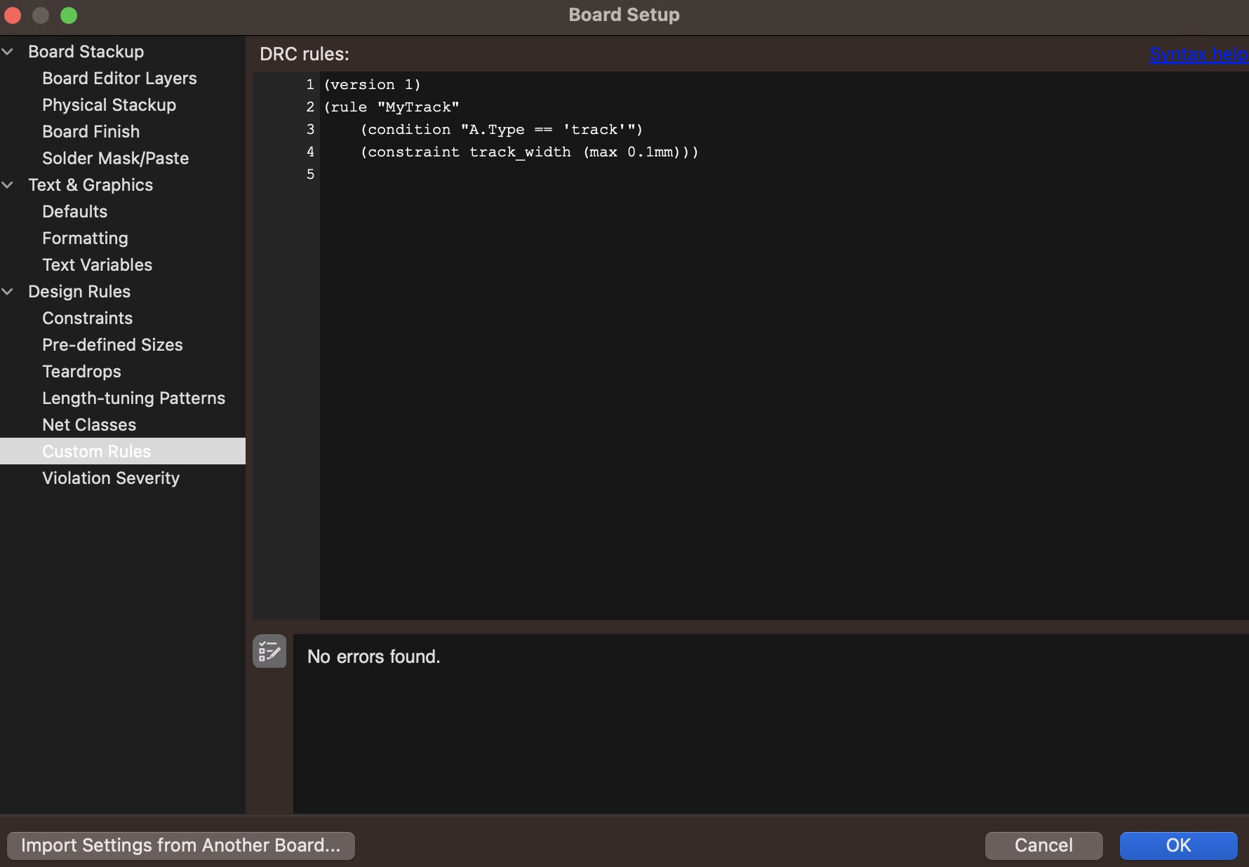 saludpcb.com
KiCad 8 Custom PCB Design Rules | SaludPCB
Vintage Curvy PCB Traces With KiCad 7 - Element14 Community
 community.element14.com
Vintage Curvy PCB Traces with KiCad 7 - element14 Community
Create Custom Pcb Designs With Kicad Expertise By Pcbprof | Fiverr
 www.fiverr.com
Create custom pcb designs with kicad expertise by Pcbprof | Fiverr
Curved Traces Made With KiCad 5.99 : R/KiCad
 www.reddit.com
Curved Traces made with KiCad 5.99 : r/KiCad
How To Design Coplanar Waveguide With Ground In Your PCB: Mastering
 hcjm-pcba.com
How to Design Coplanar Waveguide with Ground in Your PCB: Mastering ...
Macro Photograph Of Red PCB With Curved Traces And Gold Vias Stock
 www.dreamstime.com
Macro Photograph of Red PCB with Curved Traces and Gold Vias Stock ...
Melting KiCad - Mitxela.com
 mitxela.com
Melting KiCad - mitxela.com
Melting KiCad – Making Curved Traces « Adafruit Industries – Makers
 blog.adafruit.com
Melting KiCad – making curved traces « Adafruit Industries – Makers ...
Kicad PCB: How To Understand It ? - Jarnistech
 www.jarnistech.com
Kicad PCB: How to Understand It ? - Jarnistech
Mastering KiCAD: Open-Source PCB Design For Beginners | Datafloq News
 datafloq.com
Mastering KiCAD: Open-Source PCB Design for Beginners | Datafloq News
Curved Traces In KiCad 5.99
 kbd.news
Curved traces in KiCad 5.99
How To Design Coplanar Waveguide With Ground In Your PCB: Mastering
 hcjm-pcba.com
How to Design Coplanar Waveguide with Ground in Your PCB: Mastering ...
Vintage Curvy PCB Traces With KiCad 7 - Element14 Community
 community.element14.com
Vintage Curvy PCB Traces with KiCad 7 - element14 Community
Create Custom Pcb Designs With Kicad Expertise By Pcbprof | Fiverr
 www.fiverr.com
Create custom pcb designs with kicad expertise by Pcbprof | Fiverr
KiCad 8 Custom PCB Design Rules | SaludPCB
 saludpcb.com
KiCad 8 Custom PCB Design Rules | SaludPCB
What Are The Steps In Designing The Custom PCB? – Hillman Curtis
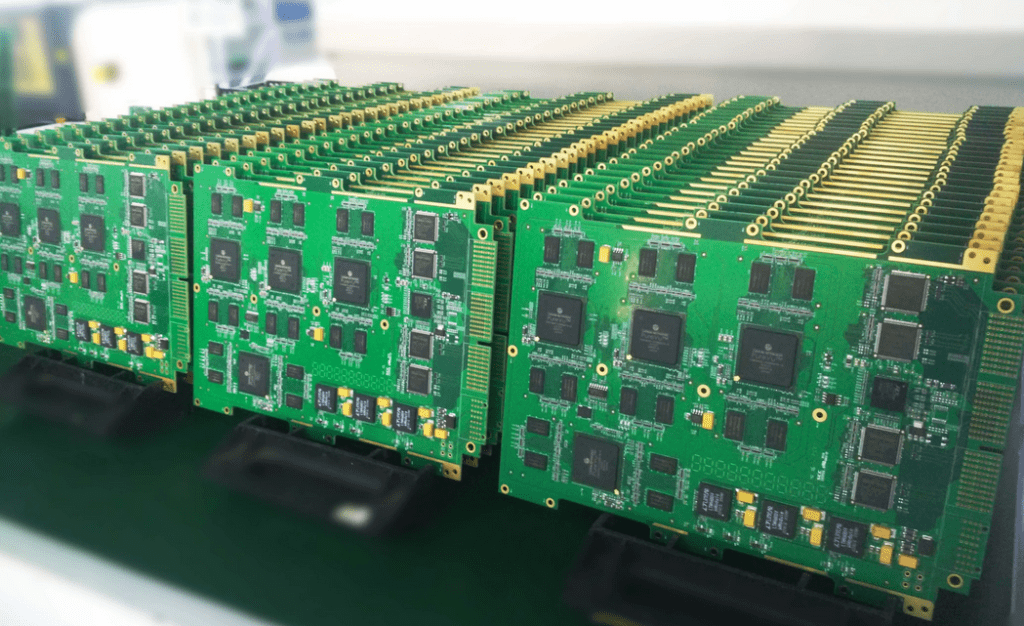 hillmancurtis.com
What are the Steps in Designing the Custom PCB? – Hillman Curtis ...
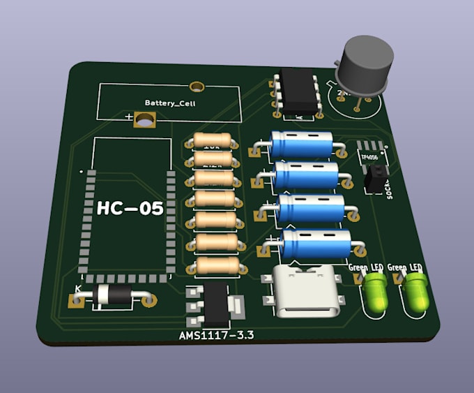
Keyboard PCB Design With KiCad: A Comprehensive Guide – Hillman Curtis
 hillmancurtis.com
Keyboard PCB Design with KiCad: A Comprehensive Guide – Hillman Curtis ...
Kicad 2 Layer PCB Design: Tips And Best Practices – Hillman Curtis
 hillmancurtis.com
Kicad 2 Layer PCB Design: Tips and Best Practices – Hillman Curtis ...
How To Design Coplanar Waveguide With Ground In Your PCB: Mastering
 hcjm-pcba.com
How to Design Coplanar Waveguide with Ground in Your PCB: Mastering ...
How To Design Coplanar Waveguide With Ground In Your PCB: Mastering
 hcjm-pcba.com
How to Design Coplanar Waveguide with Ground in Your PCB: Mastering ...
How To Design Coplanar Waveguide With Ground In Your PCB: Mastering
 hcjm-pcba.com
How to Design Coplanar Waveguide with Ground in Your PCB: Mastering ...
How To Design Coplanar Waveguide With Ground In Your PCB: Mastering
 hcjm-pcba.com
How to Design Coplanar Waveguide with Ground in Your PCB: Mastering ...
A Robot With A Pcb In Its Hands Is Working On A Circuit Board, Uhd
 www.dreamstime.com
A Robot with a Pcb in Its Hands is Working on a Circuit Board, Uhd ...
Raspberry Pi Pico (RP2040) Schematic & PCB Design In KiCAD – DeepBlue
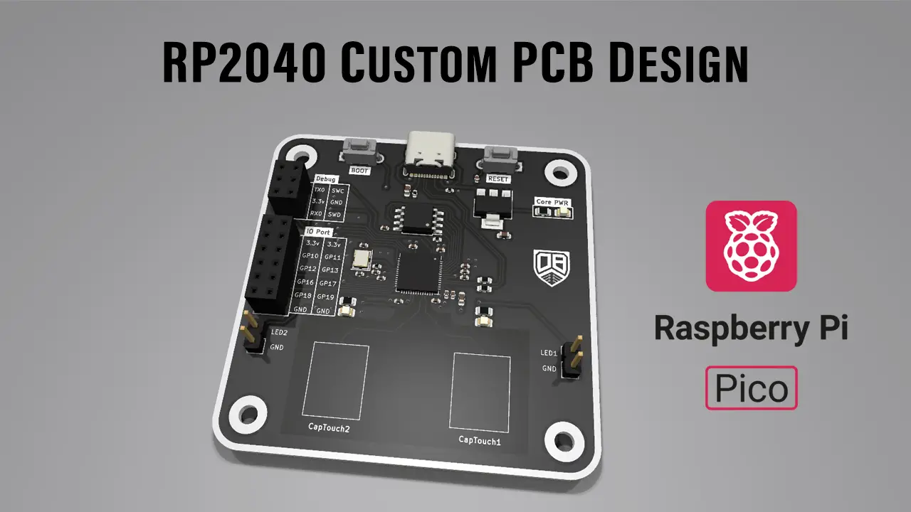 deepbluembedded.com
Raspberry Pi Pico (RP2040) Schematic & PCB Design in KiCAD – DeepBlue
How To Design Coplanar Waveguide With Ground In Your PCB: Mastering
 hcjm-pcba.com
How to Design Coplanar Waveguide with Ground in Your PCB: Mastering ...
How To Design Coplanar Waveguide With Ground In Your PCB: Mastering
 hcjm-pcba.com
How to Design Coplanar Waveguide with Ground in Your PCB: Mastering ...
Melting KiCad – Making Curved Traces « Adafruit Industries – Makers
 blog.adafruit.com
Melting KiCad – making curved traces « Adafruit Industries – Makers ...
How to design coplanar waveguide with ground in your pcb: mastering .... Melting kicad. A robot with a pcb in its hands is working on a circuit board, uhd ...